Previous Next

    LXD31K4 │ 4 通道 16 位元 ADC/ DAC │ 市場上唯一提供 LVDS 數位訊號介面

    產品應用

    • MIMO Applications
    • Radar waveform generators and receivers
    • Digital Beam Forming
    • Medical systems
    • Telecommunicaton systems
    • Experimental Physics
    • Analog record and playback systems
    • Aerospace and test instrumentation
    • Software defined radio (SDR)

    四通道 MIMO FMC 模組

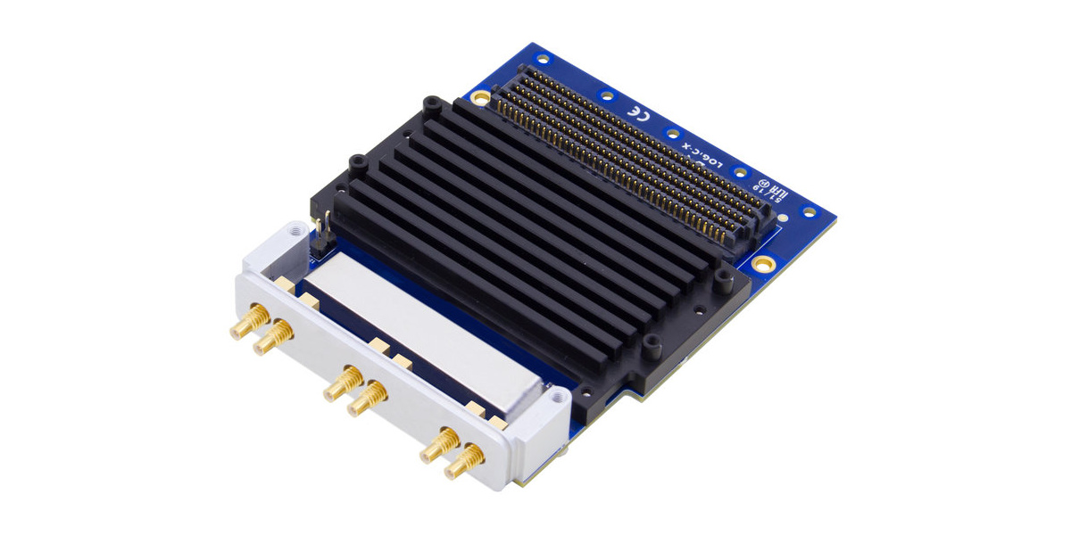
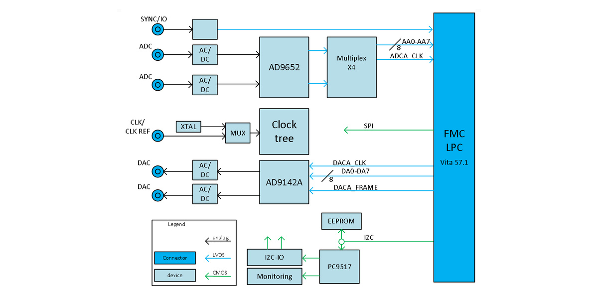
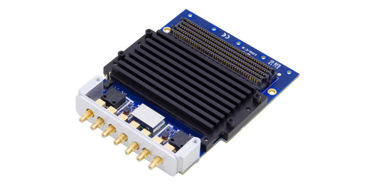
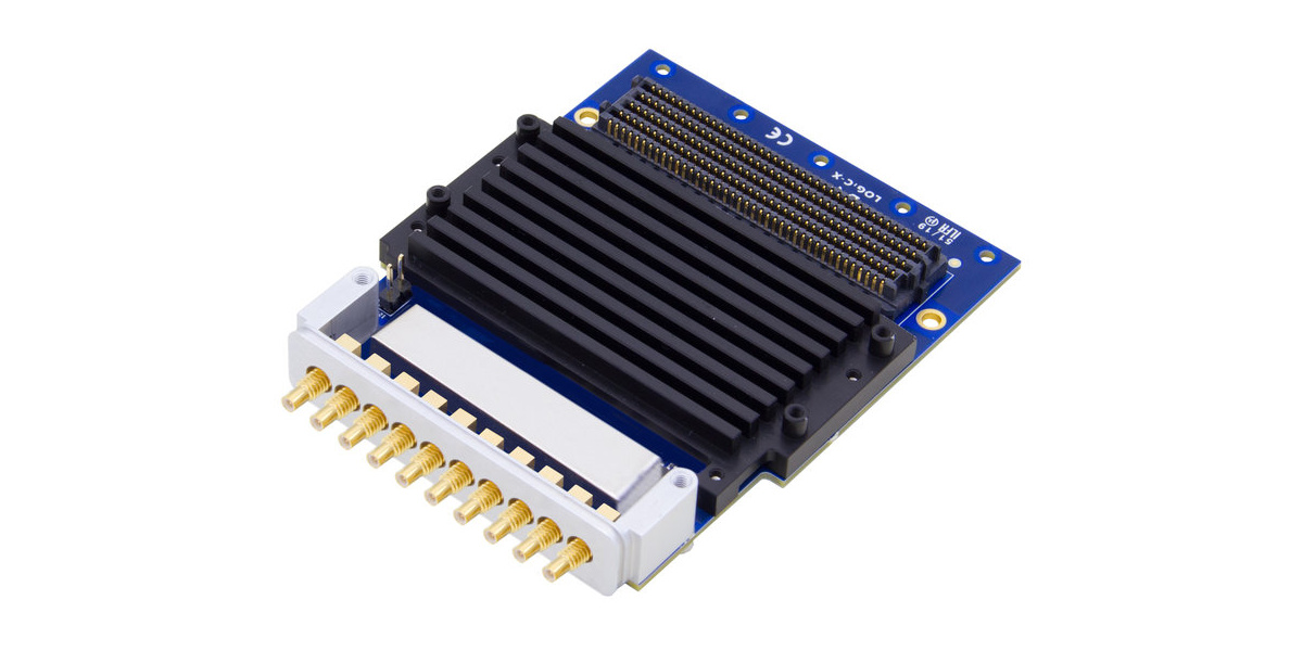
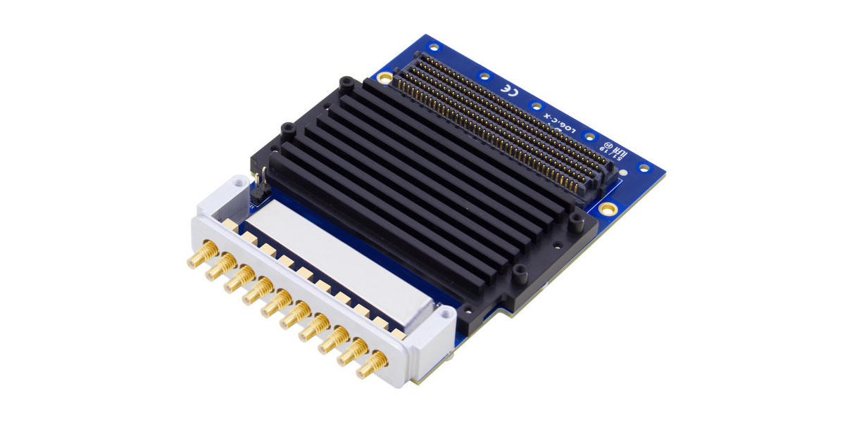
    The LXD31K4 provides four 16-bit A/D channels with up to 310 Msps data rate and four 16-bit D/A channels with up to 310 Msps data rate with a 1.24 Gsps update rate. This is the only FMC card on the market to offer this number of channels with LVDS digital signalling interfaces. The design is based on the Analog devices AD9652 analog to digital converters and the Analog devices AD9142A digital to analog converters.

    類比輸入/輸出

    Depending on the application requirements it is possible to order the LXD31K4 with either a DC coupled or an AC coupled analog front end. The DC coupled interface is meant for signal acquisitions and playback in the first Nyquist zone while the AC coupled inputs also offers the option for signal acquisition and playback in the second Nyquist zone.

    16位元

    Both the ADC and DAC offer 16-bits resolution further contributing to achieve best in class signal to noise ratios.

    LVDS訊號

    Both the ADC and DAC device make use of LVDS signaling for their data interfaces. This allows easy integration of the LXD31K4 into user FPGA designs without the need to acquire expensive and complex JESD204B interface cores. Furthermore the pinout is chosen in a way that it will work on most of the partial implementations of the high pin count connectors on Xilinx development boards as well as the Logic-X FPGA FMC carrier boards.

    時脈功能

    The onboard low noise clock generator ensures easy integration into small single board systems as well as standalone operation. For larger systems it is possible to easily synchronize multiple boards by providing an external reference clock. This is a special feature offered by the onboard clock PLL.


    產品規格

    Number of analog input channels:4
    Number of analog output channels:4
    Front panel IO connector type:SSMC/ MMCX
    Front panel IO type:ADC/DAC
    Form Factor:FMC - High pin count (HPC)

    Analog input specification

    Input coupling:AC coupling/ DC Coupling
    Input maximum sample rate:310 Msps
    Input number of bits:16 bits resolution 
    Impedance:50 Ω 
    Input bandwidth AC coupled:10 MHz - 400 MHz
    Input bandwidth DC coupled:DC - 200 MHz
    Input AC full scale power:+6 dBm
    Input DC full scale power:+12 dBm

    Analog output specifications

    Output coupling:AC coupling/ DC Coupling
    Output maximum sample rate:310 Msps (1210 MHz update rate)
    Output number of bits:16 bits resolution
    Impedance:50 Ω
    Output impedance AC coupled:10 MHz - 400 MHz
    Output bandwidth DC coupled:DC - 200 MHz
    Output AC full scale power:+6 dBm
    Output DC full scale power:+12 dBm

    Legislation and Environmental 

    Supported operating temperature (2選1):Commercial (0°C ~ 70°C) / Industrial (-40°C ~ 85°C) 
    Ruggedization:standard Commercial Air-cooled and Rugged Conduction- cooled
    ROHS Compliant:Yes - RoHS Phthalates Compliant 
    SVHC:Product contains no SVHC
    Country of origin:the Netherlands (Europe) (荷蘭製造生產)
    ECCN :3A002.h.1.e.

    Conformal Coating (2選1):No coating / Mil-I-46058-C Confomal Coating

    011 yes 128   產品文件:產品規格表
    Previous Next

    LXD31K2 │ 雙通道 16 位元 ADC/DAC FMC │ MIMO 波束成形 醫療 電信 航太應用 SDR

    產品應用

    • MIMO Applications
    • Radar waveform generators and receivers
    • Digital Beam Forming
    • Medical systems
    • Telecommunicaton systems
    • Experimental Physics
    • Analog playback systems
    • Aerospace and test instrumentation
    • Software defined radio (SDR)

    雙通道 MIMO FMC 模組

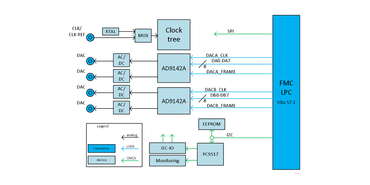
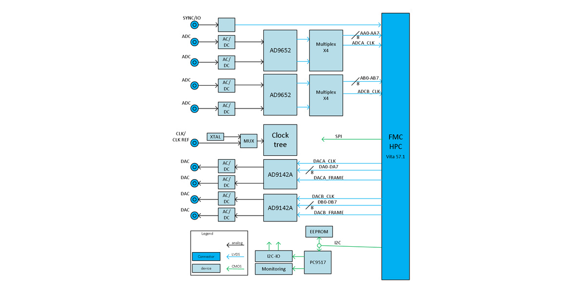
    The LXD31K2 provides two 16-bit A/D channels with up to 310 Msps data rate and two 16-bit D/A channels with up to 310 Msps data rate with a 1.24 Gsps update rate. All the data interfaces are based on LVCMOS and LVDS signalling.The design is based on the Analog devices AD9652 analog to digital converters and the Analog devices AD9142A digital to analog converters.

    類比輸入/輸出

    Depending on the application requirements it is possible to order the LXD31K2 with either a DC coupled or an AC coupled analog front end. The DC coupled interface is meant for signal acquisitions and playback in the first Nyquist zone while the AC coupled inputs also offers the option for signal acquisition and playback in the second Nyquist zone.

    16位元

    Both the ADC and DAC offer 16-bits resolution further contributing to achieve best in class signal to noise ratios.

    LVDS訊號功能

    Both the ADC and DAC device make use of LVDS signaling for their data interfaces. This allows easy integration of the LXD31K2 into user FPGA designs without the need to acquire expensive and complex JESD204B interface cores. Thanks to the low pin count implementation the LXD31K2 will work on all Xilinx development boards as well as the Logic-X FPGA FMC carrier boards.

    時脈功能

    The onboard low noise clock generator ensures easy integration into small single board systems as well as standalone operation. For larger systems it is possible to easily synchronize multiple boards by providing an external reference clock. This is a special feature offered by the onboard clock PLL.


    產品規格

    Number of analog input channels:2
    Number of analog output channels:2
    Front panel IO connector type:SSMC/ MMCX
    Front panel IO type:ADC/DAC
    Form Factor:FMC - Low pin count (LPC)

    Analog input specification

    Input coupling:AC or DC coupled
    Input maximum sample rate:310 Msps
    Input number of bits:16 bits resolution
    Impedance:50 Ω
    Input bandwidth AC coupled:10 MHz - 400 MHz
    Input bandwidth DC coupled:DC - 200 MHz
    Input AC full scale power:+6 dBm
    Input DC full scale power:+12 dBm

    Analog output specifications

    Output coupling:AC or DC coupled
    Output maximum sample rate:310 Msps (1210 MHz update rate)
    Output number of bits:16 bits resolution
    Impedance:50 Ω
    Output impedance AC coupled:10 MHz - 400 MHz
    Output bandwidth DC coupled:DC - 200 MHz
    Output AC full scale power:+6 dBm
    Output DC full scale power:+12 dBm

    Legislation and Environmental 

    Supported operating temperature (2選1):Commercial (0°C ~ 70°C) / Industrial (-40°C ~ 85°C) 
    Ruggedization:standard Commercial Air-cooled and Rugged Conduction- cooled
    ROHS Compliant:Yes - RoHS Phthalates Compliant 
    SVHC:Product contains no SVHC
    Country of origin:the Netherlands (Europe) (荷蘭製造生產)
    ECCN :3A002.h.1.e

    Conformal Coating (2選1):No coating / Mil-I-46058-C Confomal Coating

    011 yes 128   產品文件:產品規格表
    Previous Next

    LXD20K0 │ 12 位元低延遲寬頻 DAC │ 電子戰 雷達應用 DRFM 醫療 電信應用

    產品應用

    • Electronic Warfare systems
    • Radar waveform generators and receivers
    • Advanced digital radio frequency memory (DRFM) systems
    • Medical systems
    • Telecommunicaton systems

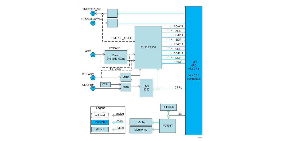
    以5.4 Gsps 解析度進行 12 位元解析度的低延遲數據擷取

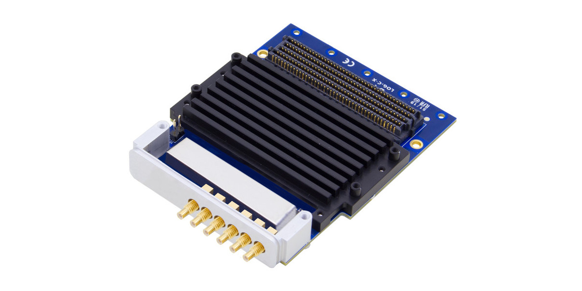
    With the LXD20K0 Logic-X provides a unique analog interface product that is based on the 12-bits low latency wide bandwidth DAC (EV12DS460) from Teledyne E2V. Multi card synchronization is supported thanks to a flexible clock tree and external synchronization trigger input.

    類比輸出

    The analog output offers a lowe latency (1.2 ns) from FPGA to RF using the EV12DS480 DAC device from E2V. The product has an output bandwidth from 0.5MHz to 6GHz. The instantaneous output bandwidth is up-to 1.35 GHz. Thanks to the unique operating modes of the EV12DS460 it is possible to place the signal into the higher Nyquist bands.

    12位元

    The DAC offers a 12-bits resolution further contributing to achieve best in class signal to noise ratios.

    低延遲

    It is possible to achieve a very low latency from the RF input to the RF output because of the LVDS connectvity to the host carrier. This can be less than 18 ns, depending on the carrier that is used.

    時脈功能

    The onboard low noise clock generator ensures easy integraton into small single channel systems as well as standalone operaton. For larger systems it is possible to directly provide the sample clock to the front panel SSMC connector or to synchronize the local clock generator to an external reference clock.


    產品規格

    Number of analog input channels:1
    Number of analog output channels:1
    Front panel IO connector type:SSMC/ MMCX
    Front panel IO type:DAC
    Form Factor:FMC - High pin count (HPC)

    Analog input specification

    Input coupling:AC coupling 
    Input maximum sample rate:310 Msps
    Input number of bits:16 bits resolution 
    Impedance:50 Ω 
    Input bandwidth AC coupled:0.5 MHz - 4.8 MHz
    Input AC full scale power:+ 8.5 dBm

    Analog output specification

    Output coupling:AC coupled
    Output maximum sample rate:2.7 Gsps (5.4 GHz update rate)
    Output number of bits:16 bits resolution
    Impedance:50 Ω
    Output impedance AC coupled:0.5 MHz - 6 GHz
    Output AC full scale power:-5 dBm (NRZ mode)

    Legislation and Environmental 

    Supported operating temperature (2選1):Commercial (0°C ~ 70°C) / Industrial (-40°C ~ 85°C) 
    Ruggedization:standard Commercial Air-cooled and Rugged Conduction- cooled
    ROHS Compliant:Yes - RoHS Phthalates Compliant 
    SVHC:Product contains no SVHC
    Country of origin:the Netherlands (Europe) (荷蘭製造生產)
    ECCN :3A002.h.1.c

    Conformal Coating (2選1):No coating / Mil-I-46058-C Confomal Coating

    011 yes 128   產品文件:產品規格表
    Previous Next

    LXD21K4 │ 4 通道 16 位元 DAC FMC │ MIMO 雷達 醫療 航太應用 SDR

    產品應用

    • MIMO Applications
    • Radar waveform generators
    • Digital Beam Forming
    • Medical systems
    • Telecommunicaton systems
    • Experimental Physics
    • Analog playback systems
    • Aerospace and test instrumentation
    • Software defined radio (SDR)

    四通道 DAC FMC 模組

    The LXD21K4 provides four 16-bit D/A channels with up to 310 Msps data rate and a 1.24 Gsps update rate. This is the only FMC card on the market to offer this number of channels with LVDS digital signalling interfaces. The design is based on the Analog devices AD9142A digital to analog converters.

    類比輸入/輸出

    Depending on the application requirements it is possible to order the LXD21K4 with either a DC coupled or an AC coupled analog front end. The DC coupled interface is meant for signal acquisitions and playback in the first Nyquist zone while the AC coupled inputs also offers the option for signal acquisition and playback in the second Nyquist zone.

    16位元

    The ADC offers 12-bits resolution further contributing to achieve best in class signal to noise ratios.

    LVDS訊號功能

    The DAC devices make use of LVDS signaling for their data interfaces. This allows easy integration of the LXD21K4 into user FPGA designs without the need to acquire expensive and complex JESD204B interface cores. Thanks to the low pin count implementation the LXD21K4 will work on all Xilinx development boards as well as the Logic-X FPGA FMC carrier boards.The DAC devices make use of LVDS signaling for their data interfaces. This allows easy integration of the LXD21K4 into user FPGA designs without the need to acquire expensive and complex JESD204B interface cores. Thanks to the low pin count implementation the LXD21K4 will work on all Xilinx development boards as well as the Logic-X FPGA FMC carrier boards.

    時脈功能

    The onboard low noise clock generator ensures easy integration into small single board systems as well as standalone operation. For larger systems it is possible to easily synchronize multiple boards by providing an external reference clock. This is a special feature offered by the onboard clock PLL.


    產品規格

    Number of analog input channels:4
    Front panel IO connector type:SSMC/ MMCX
    Front panel IO type:DAC
    Form Factor:FMC - Low pin count (LPC)

    Analog output specification

    Output maximum sample rate:310 Msps (1210 MHz update rate)
    Output number of bits:16 bits resolution
    Impedance:50 Ω
    Output impedance AC coupled:10 MHz - 400 MHz
    Output bandwidth DC coupled:DC - 200 MHz
    Output AC full scale power:+6 dBm
    Output DC full scale power:+12 dBm

    Legislation and Environmental 

    Supported operating temperature (2選1):Commercial (0°C ~ 70°C) / Industrial (-40°C ~ 85°C) 
    Ruggedization:standard Commercial Air-cooled and Rugged Conduction- cooled
    ROHS Compliant:Yes - RoHS Phthalates Compliant 
    SVHC:Product contains no SVHC
    Country of origin:the Netherlands (Europe) (荷蘭製造生產)
    ECCN :3A002.h.1.e

    Conformal Coating (2選1):No coating / Mil-I-46058-C Confomal Coating

    011 yes 128   產品文件:產品規格表
    Previous Next

    LXD11K8 │ 8 通道 16 位元 ADC │ MIMO 波束成形 雷達應用 電信系統 航太應用 SDR

    產品應用

    • MIMO Applications
    • Radar waveform receivers
    • Digital Beam Forming
    • Medical systems
    • Telecommunicaton systems
    • Experimental Physics
    • Analog playback systems
    • Aerospace and test instrumentation
    • Software defined radio (SDR)

    8 通道 16 位元 ADC FMC 模組

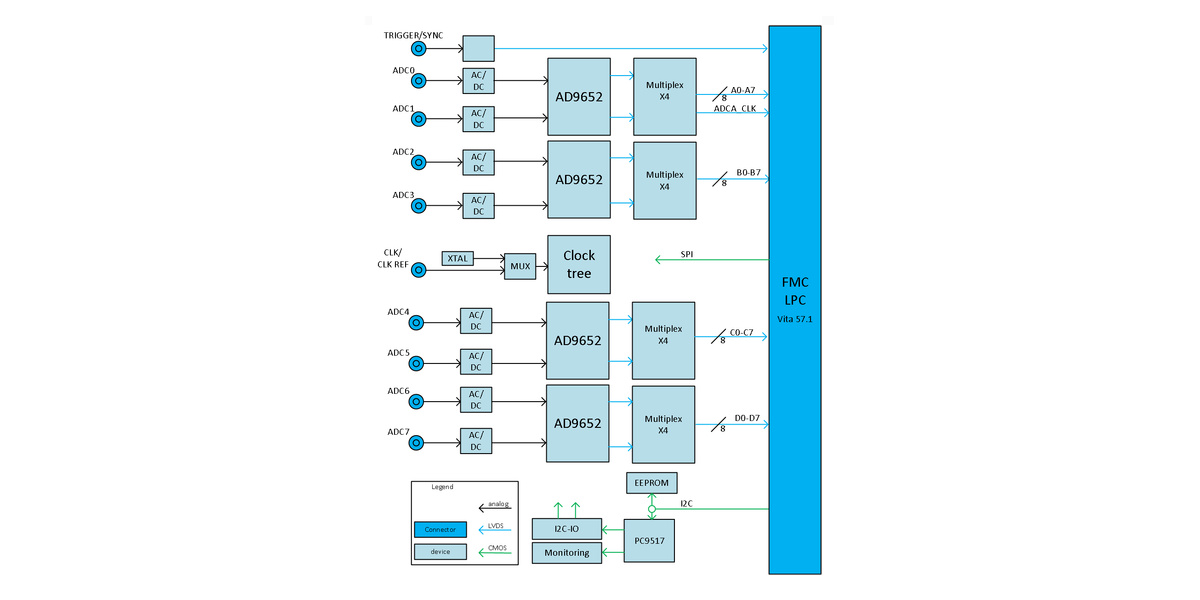
    The LXD11K8 provides eight 16-bit A/D channels with up to 310 Msps data rate. All the data interfaces are based on LVCMOS and LVDS signalling. The design is based on the Analog devices AD9652 analog to digital converters.

    類比輸入/輸出

    Depending on the application requirements it is possible to order the LXD11K8 with either a DC coupled or an AC coupled analog front end. The DC coupled interface is meant for signal acquisitions in the first Nyquist zone while the AC coupled inputs also offers the option for signal acquisition in the second Nyquist zone.

    16位元

    The ADCs offer 16-bits resolution further contributing to achieve best in class signal to noise ratios.

    LVDS訊號功能

    The ADC devices make use of LVDS signaling for their data interfaces. This allows easy integration of the LXD11K8 into user FPGA designs without the need to acquire expensive and complex JESD204B interface cores. Furthermore the low pin count implementation make sure the card can be used on all Xilinx development boards as well as the Logic-X FPGA FMC carrier boards.

    時脈功能

    The onboard low noise clock generator ensures easy integration into small single board systems as well as standalone operation. For larger systems it is possible to easily synchronize multiple boards by providing an external reference clock. This is a special feature offered by the onboard clock PLL.


    產品規格

    Number of analog input channels:8
    Front panel IO connector type:SSMC or MMCX
    Front panel IO type:ADC
    Form Factor:FMC - High pin count (HPC)

    Analog input specification

    Input coupling:AC or DC coupled
    Input maximum sample rate:310 Msps
    Input number of bits:16 bits resolution
    Impedance:50 Ω
    Input bandwidth AC coupled:10 MHz - 400 MHz
    Input bandwidth DC coupled:DC - 200 MHz
    Input AC full scale power:+6 dBm
    Input DC full scale power:+12 dBm

    Legislation and Environmental

    Supported operating temperature:Commercial (0°C ~ 70°C) and Industrial (-40°C ~ 85°C)
    Ruggedization:standard Commercial Air-cooled and Rugged Conduction- cooled
    ROHS Compliant:Yes - RoHS Phthalates Compliant
    SVHC:Product contains no SVHC (15-May-2020)
    Country of origin:the Netherlands (Europe)
    Tariff Number (HS code):854231 - Electronic printed circuits
    ECCN:3A002.h.1.e

    011 yes 128   產品文件:產品規格表
     

    和澄科技 Haley Technology

    電話 │ 886-3-5790380
    傳真 │ 886-3-5790370
    信箱 │ sales@haleytech.com
    地址 │ 新竹市關新路27號18樓之2


    M有任何問題嗎? Line 我們最快! 

    產品搜尋