Previous Next

    Virtex UltraScale+ 系列 │ quad XCVU19P 套裝系統

    Product Summary

    XCVU19P rototyping System - The proFPGA quad XCVU19P system is a complete and modular multi FPGA solution, which meets highest requirements in the area of FPGA based Prototyping. It addresses customers who need a scalable and flexible high speed ASIC Prototyping solution for early software development and real time system verification. The innovative system concept offers highest flexibility and reusability, reconfigurability for several projects, which guarantees the best return on invest.rn on invest.

    Highest Flexibility

    The system architecture is based on a modular and scalable system concept. The FPGAs are assembled on dedicated FPGA modules, which will be plugged on the proFPGA uno, duo or quad mother board. This offers the highest flexibility to use for example different FPGA types in one system or to scale a system in increments of one FPGA. The user has nearly 100% access to all available I/Os of the FPGA, which gives him maximum freedom regarding the FPGA inter connection structure. This way the prototyping system can be adapted in the best way to any user design. Furthermore the system offers a total of 56 extension sites on the top and bottom site for standard proFPGA or user specific extension boards like DDR-4 memory, PCIe gen4, Gigabit Ethernet, QSFP28 or other high performance interface and interconnection boards.

    Maximum Performance

    The well designed boards of the proFPGA system are optimized and trimmed to guarantee best signal integrity and to achieve highest performance. The latest Xilinx® Virtex® UltraScale+™ FPGA technology, high-speed PCB design with delay matched signal lines and high-end PCB materials allow the new proFPGA platforms to offer best signal integrity and to run up to 30% faster than the previous proFPGA XCVU440-based product generation. Through standard I/Os the system achieves a single-ended point-to-point performance of about 1.4 Gbps and via the Multi Gigabit Transceivers (MGTs) even up to 25 Gbps.

    Biggest Capacity

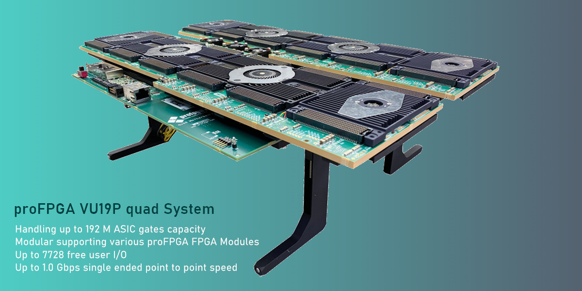
    Equipped with up to 4 Xilinx Virtex® UltraScale+™ 19P FPGA modules, the proFPGA quad system can handle up to 192 M ASIC gates on only one board. Due to the fact, that multiple proFPGA quad or duo systems can be connected to an even larger system, there is an unli- mited scalability and no theoretical maximum in capacity.

    Very User Friendly

    The proFPGA prototyping system provides an extensive set of features and tools, like remote system configuration, integrated self and performance test, automatic board detection, automatic I/O voltage programming, system scan and safety mechanism, which simplifies the usage of the FPGA based system tremendously.


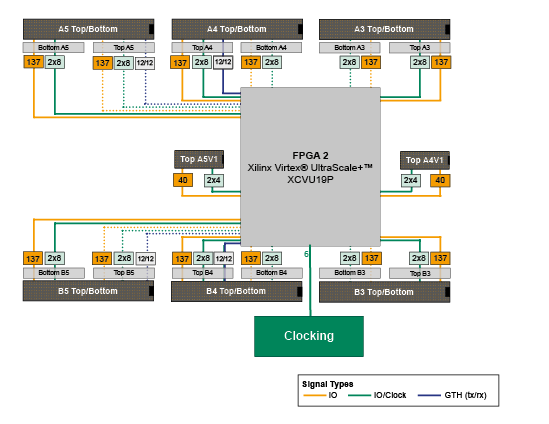
    System Architechture
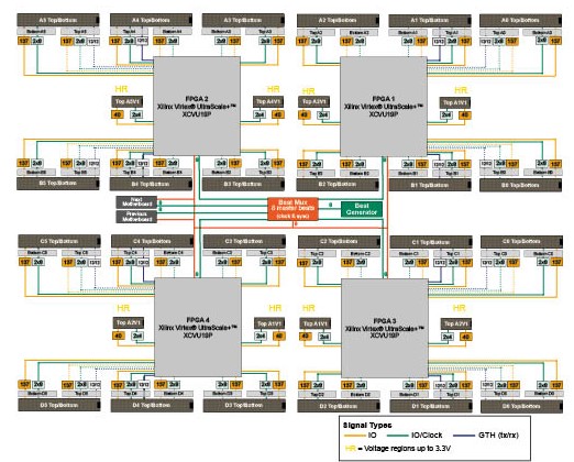
     

    Configuration 


    proFPGA quad UltraScale+ XCVU19P FPGA Prototyping System Configurations

    proFPGA quad XCVU19P FM1

    proFPGA quad XCVU19P FM2

    proFPGA quad XCVU19P FM3

    proFPGA quad XCVU19P FM4

    Extension Sites

    14

    28

    42

    56

    FPGA Modules

    1

    2

    3

    4

    FPGAType

    Xilinx Virtex UltraScale+ XCVU19P

    Xilinx Virtex UltraScale+ XCVU19P

    Xilinx Virtex UltraScale+ XCVU19P

    Xilinx Virtex UltraScale+ XCVU19P

    Logic Capacity (ASIC Gates)

    48 M

    96 M

    134 M

    192 M

    FPGA Memory

    75,9 Mbit

    151,8 Mbit

    227,7 Mbit

    303,6 Mbit

    I/O Resources

    1932

    3864

    5796

    7728

    High Speed I/O Transceivers

    48

    96

    144

    192

    Adjustable Voltage Regions

    14

    28

    42

    56

    Interconnections

    flexible

    flexible

    flexible

    flexible

    Clock Inputs

    104

    208

    312

    416

    Global Clocks

    8/x-derived

    8/x-derived

    8/x-derived

    8/x-derived

    Order Code

    PROF-QUAD-XCVU19P-FM1

    PROF-QUAD-XCVU19P-FM2

    PROF-QUAD-XCVU19P-FM3

    PROF-QUAD-XCVU19P-FM4


    011 yes 128   產品文件:
    20171115 04   產品編號:PROF-QUAD-XCVU19P-FM1 / PROF-QUAD-XCVU19P-FM2 / PROF-QUAD-XCVU19P-FM3 / PROF-QUAD-XCVU19P-FM4
    Previous Next

    Virtex UltraScale+ 系列 │ duo XCVU19P 套裝系統

    Product Summary

    The proFPGA duo XCVU19P system is a complete and modular multi-FPGA solution, which meets highest requirements in the area of FPGA based Prototyping. It addresses customers who need a scalable and flexible high speed ASIC Prototyping solution for early software development and real time system verification. The innovative system concept offers highest flexibility and reusability reconfigurability for several projects, which guarantees the best return on investment.

    Highest Flexibility

    The system architecture is based on a modular and scalable single-chip concept. The FPGAs are assembled on dedicated FPGA modules, which will be plugged on the proFPGA uno, duo or quad motherboard. This offers the highest flexibility to use for example different FPGA types in one system or to scale a system in increments of one FPGA. The user has access to almost all I/Os of the FPGA, which gives him maximum freedom regarding the FPGA interconnection structure. This way the prototyping system can be adapted in the best way to any user design. Furthermore the system offers a total of 56 extension sites on the top and bottom site for standard or user specific extension boards like DDR4 memory, PCIe gen4, Gigabit Ethernet, USB 3.0, QSFP28, or other high speed interface and interconnect boards.

    Maximum Performance

    The well designed boards of the proFPGA system are optimized and trimmed to guarantee best signal integrity and to achieve highest performance. The high speed boards together with specific high speed connectors allow a maximum point-to-point speed of up to 1.0 Gbps single ended over the standard FPGA I/Os and up to 28 Gbps differential over the high speed serial transceivers of the FPGA. This performance combined with the high interconnection flexibility allows the designer to run his design at the highest possible speed in the proFPGA system.

    Biggest Capacity

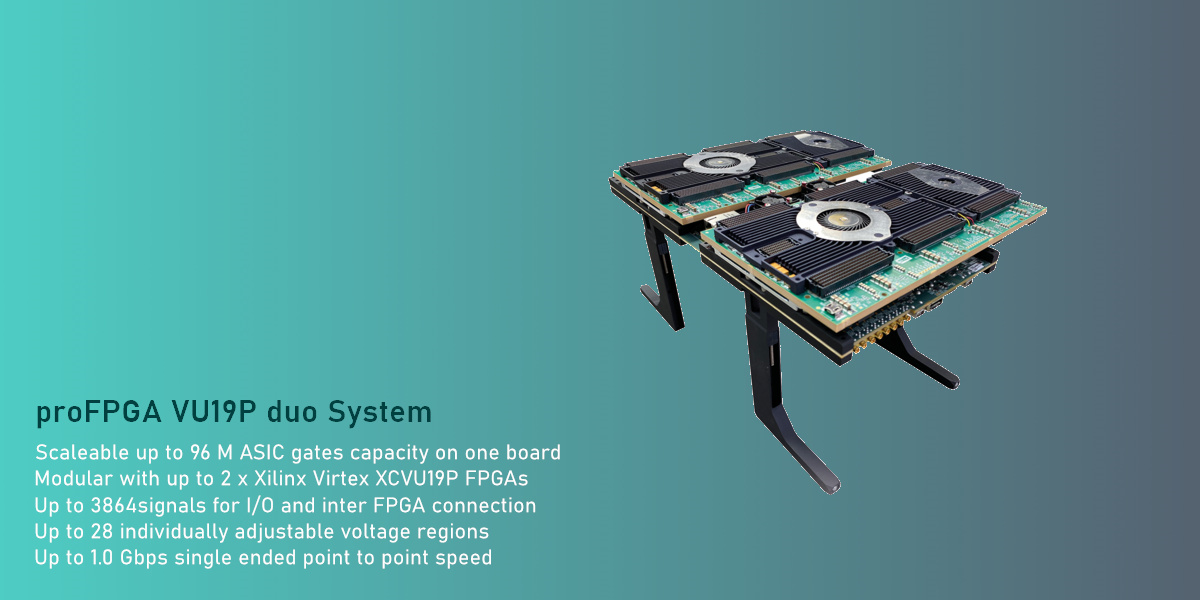
    Equipped with up to two Xilinx Virtex® UltraScale+TM VU19P FPGA modules, the proFPGA duo system can handle up to 96 M ASIC gates on only one board. Due to the fact, that multiple proFPGA quad or duo systems can be connected to even larger systems, there is an unlimited scalability and no theoretical maximum in capacity.

    Very User Friendly

    The proFPGA prototyping system provides an extensive set of features and tools, like remote system configuration, integrated self and performance test, automatic board detection, automatic I/O voltage programming, system scan and safety mechanism, which simplifies the usage of the FPGA based system tremendously.

    Specification

    • FPGAs: Up to 4 x Xilinx Virtex XCVU19P FPGA Modules
    • Capacity: Up to 192 Million ASIC gates on one board (48 Million ASIC gates per FPGA Module)   
    • Signaling rate: Up to 1.0 Gbps single ended (standard I/O)/ up to 12.5 Gbps (MGT) differential
    • Extension sites: Up to 16 extension sites with high speed connectors
    • I/O resources:Overall 7728 signals for I/O and inter FPGA connection
      • 1932 free I/Os per FPGA Module
        • 6 x 153 I/Os and 2 x 48 I/Os to top side connectors
        • 6 x 153 I/Os bottom side connector
        • Single-ended or differential
    • High Speed I/O transceivers
      • 96 dedicated MGTs running up to 16 Gbps
      • 48 MGTs (up to 28 Gbps) per FPGA Module
    • FPGAs interconnections: Flexible via high-speed interconnection boards or cables
    • Voltage regions
      • 28 individually adjustable I/O voltage regions
        • 14 individually adjustable voltage regions per FPGA Module
        • Stepless from 1.2V up 1.8V
        • Automated detection of daughter cards and setting of right voltages
    • Configuration
      • With host software via Ethernet, USB 2.0, PCIe or standalone over USB stick or JTAG
    • Clock Management
      • 208 differential external clock inputs
        • 104 differential clock inputs per FPGA Module
          • 12 x 8 and 2 x 4 differential clock inputs per connector
          • Run-time configurable local clocks8 global clock and sync signal inputs per motherboard
          • Fully synchronous derived clocks with sync signals
    • Data exchange : On board DMBI (Device Message Box Interface)
    • Data exchange rate:
      • Ethernet (up to 100 Mbps)
      • USB (480 Mbps)
      • PCIe (up to 3.5 Gbps)
    • Power: External (optional) ATX Power Supply (12 V, 24 - 35 A output)


    System Architechture

    (原廠尚未釋出)


    Configuration 

    proFPGA quad UltraScale+  XCVU19P FPGA Prototyping System Configurations

    proFPGA duo XCVU19P FM1

    proFPGA duo XCVU19P FM2

    Extension Sites

    14

    28

    FPGA Modules

    1

    2

    FPGAType

    Xilinx Virtex® UltraScale+™ XCVU19P

    Xilinx Virtex® UltraScale+™ XCVU19P

    Logic Capacity (ASIC Gates)

    48 M

    96 M

    FPGA Memory

    75,9 Mbit

    151,8 Mbit

    I/O Resources

    1932

    3864

    High Speed I/O Transceivers

    48

    96

    Adjustable Voltage Regions

    14

    28

    Interconnections

    flexible

    flexible

    Clock Inputs

    104

    208

    Global Clocks

    8/x-derived

    8/x-derived

    Order Code

    PROF-QUAD-XCVU19P-FM1

    PROF-QUAD-XCVU19P-FM2


    011 yes 128   產品文件:
    20171115 04   產品編號:PROF-QUAD-XCVU19P-FM1 / PROF-QUAD-XCVU19P-FM2 
    Previous Next

    Intel Stratix 10 系列 │ quad GX 10M 套裝系統 ( 2020 全新上市)

    New Intel Stratix 10 GX 10M FPGA Prototyping System

    Product Summary
    The proFPGA quad 10 GX 10M system is a complete and modular multi FPGA Prototyping solution, which meets highest requirements in the area of FPGA based Prototyping. It addresses customers who need a scalable and flexible high speed ASIC Prototyping solution for early software development and real time system verification. The innovative system concept offers highest flexibility and reusability, reconfigurability for several projects, which guarantees the best return on invest.

    Highest Flexibility
    The system architecture is based on a modular and scalable system concept. The FPGAs are assembled on dedicated FPGA modules, which will be plugged on the proFPGA motherboard. This offers the highest flexibility to use for example different FPGA types in one system or to scale a system in increments of one FPGA. The user has nearly 100% access to all available I/Os of the FPGA, which gives him maximum freedom regarding the FPGA inter connection structure. This way the prototyping system can be adapted in the best way to any user design. Furthermore the system offers a total of 32 extension sites on the top and bottom site for standard proFPGA or user specific extension boards like DDR4 memory, PCIe gen1/2/3/4, Gigabit Ethernet, USB 3.0, QSFP+ or other high performance interface and interconnection boards.

    Maximum Performance
    The well designed boards of the proFPGA system are optimized and trimmed to guarantee best signal integrity and to achieve highest performance. The high speed boards together with specific high speed connectors allow a maximum point to point speed of up to 1.0 Gbps single ended over the standard FPGA I/O and up to 17.4 Gbps differential over the high speed serial transceivers of the FPGA. This performance combined with the high interconnection flexibility allows the designer to run his design at maximum speed in the proFPGA system.

    Biggest Capacity
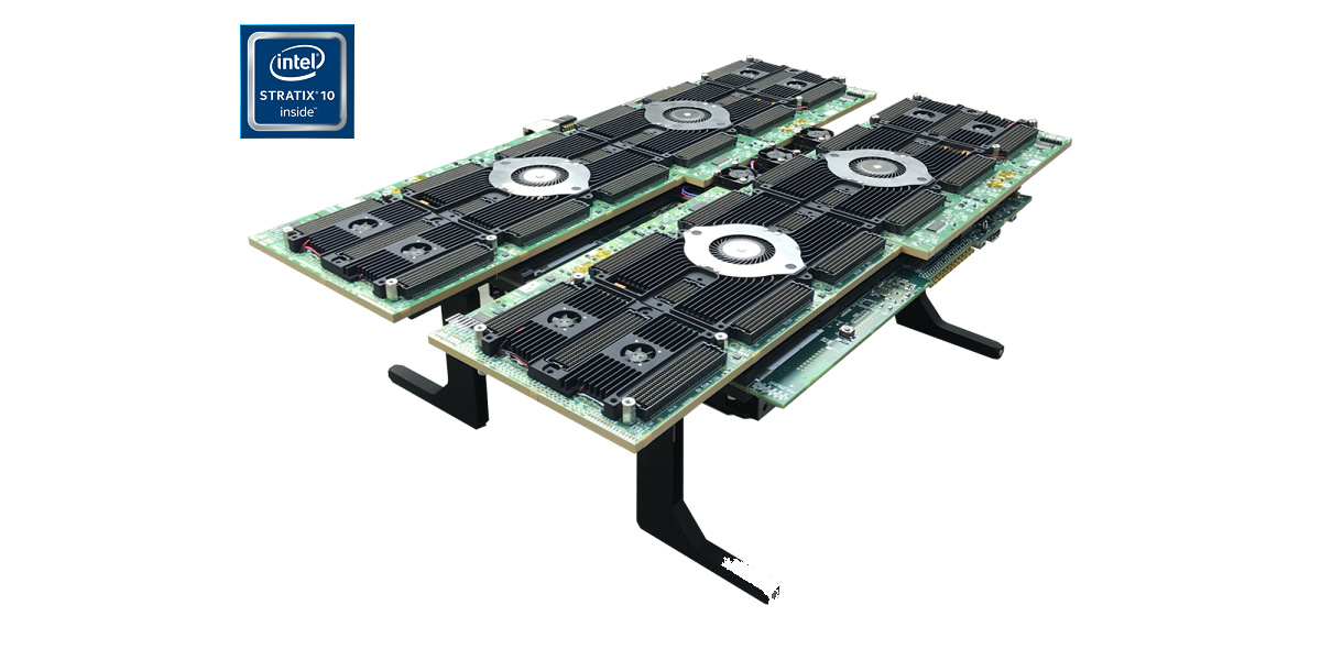
    Equipped with up to four Intel® Stratix 10 GX 10M FPGA modules, the proFPGA quad system can handle up to 240 M ASIC gates on only one board. Due to the fact, that multiple proFPGA quad or duo systems can be connected to an even larger system, there is an unli- mited scalability and no theoretical maximum in capacity.

    Very User Friendly
    The proFPGA prototyping system provides an extensive set of features and tools, like remote system configuration, integrated self and performance test, automatic board detection, automatic I/O voltage programming, system scan and safety mechanism, which simplifies the usage of the FPGA based system tremendously.

    Specification 

    FPGSs

    • Up to 4 x Intel® Stratix® 10 GX 10M FPGA Modules


    Capacity

    • Up to 240 Million ASIC gates on one board (60 Million ASIC gates per FPGA Module)


    FPGA-internal memory

    • Up to 1012 Mbit on one board (253 Mbits per FPGA Module)


    Signaling rate

    • Up to 1.4 Gbps (standard I/O)/ up to 17.4 Gbps differential


    Extension sites

    • Up to 64 extension sites with high speed connectors


    I/O resources

    • Overall 8304 signals for I/O and inter FPGA connection
      • 2076 free I/Os per FPGA Module
        • 7 x 141 to top side connectors
        • 2 x 51 to top side connectors
        • 7 x 141 to bottom side connectors
    • Single-ended or differential


    High Speed I/O transceivers

    • 192 dedicated high speed serial transceivers running up to 17.4 Gbps
      • 48 high speed serial transceivers per FPGA Module


    FPGAs interconnections

    • Flexible via high-speed interconnection boards or cables


    Voltage regions

    • 64 individually adjustable I/O voltage regions
      • 16 individually adjustable voltage regions per FPGA Module
      • Stepless from 1.2 up 1.8V
    • Automated detection of daughter card and adjustment of right voltage


    Configuration

    • With host software via Ethernet, USB 2.0, PCIe or standalone over USB stick or JTAG


    Clocking

    • 336 differential external clock inputs
      • 84 differential clock inputs per FPGA Module
      • 6 differential clock inputs per connector
    • Run-time configurable local clocks
    • 6 global clock and sync signal inputs per motherboard
    • X fully synchronous derived clocks with sync signals


    Data exchange

    • On board DMBI (Device Message Box Interface)
    • Data exchange rate:
    • Ethernet (up to 100 Mbps)
    • USB (480 Mbps)
    • PCIe (up to 3.5 Gbps)


    Power

    • External (optional) ATX Power Supply (12 V, 24 - 35 A output)


    Dimensions

    • 11.81" x 0.95" x 12.20" / 300 mm x 24 mm x 310 mm (width x height x depth)
    • 2.5 kg weight

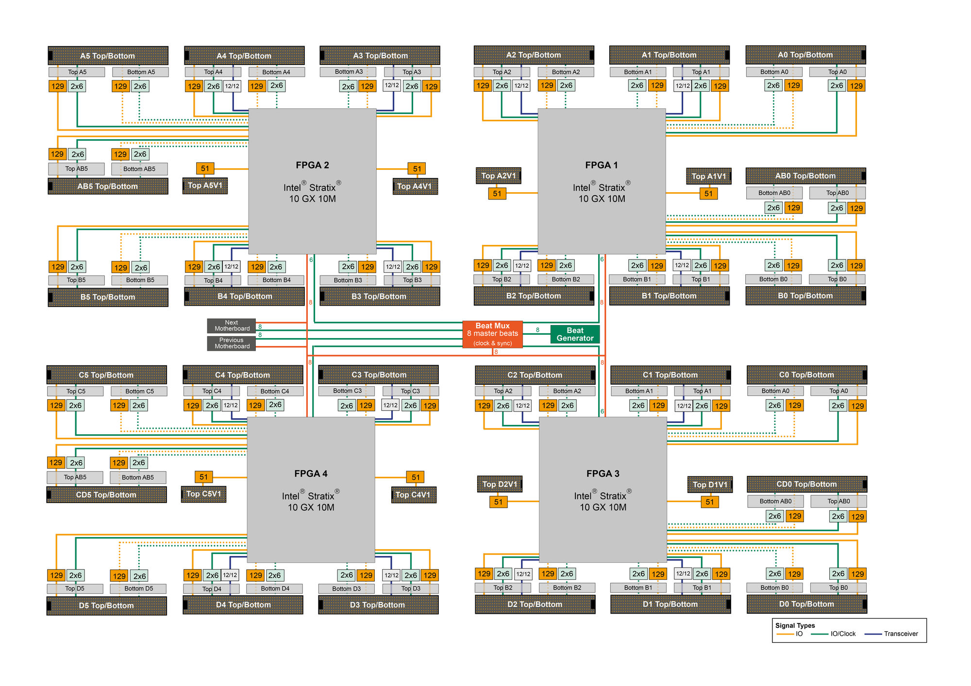
    System Architecture 

    proFPGA quad Intel® Stratix® 10 GX 10M FPGA Prototyping System Configurations
    proFPGA quad 10 GX 10M FM1 proFPGA quad 10 GX 10M FM2 proFPGA quad 10 GX 10M FM3 proFPGA quad 10 GX 10M FM4
    Extension Sites 16 32 48 64
    FPGA Modules 1 2 3 4
    FPGAType Intel® Stratix® 10 GX 10M Intel® Stratix® 10 GX 10M Intel® Stratix® 10 GX 10M Intel® Stratix® 10 GX 10M
    Logic Capacity (ASIC Gates) 60M 120M 180M 240M
    FPGA Memory 253 Mbit 506 Mbit 759 Mbit 1012 Mbit
    I/O Resources 2076 4152 6228 8304
    High Speed I/O Transceivers 48 96 144 192
    Adjustable Voltage Regions 16 32 48 64
    Interconnections flexible flexible flexible flexible
    Clock Inputs 84 + 6 168 + 6 252 + 6 336 + 6
    Global Clocks 8/x-derived 8/x-derived 8/x-derived 8/x-derived
    Order Code PROF-QUAD-10GX10M-FM1 PROF-QUAD-10GX10M-FM2 PROF-QUAD-10GX10M-FM3 PROF-QUAD-10GX10M-FM4


    20171115 04 產品文件:產品型錄(EN)  proFPGA 產品總覽 (EN)    
    011 yes 128  產品編號: PROF-QUAD-10GX10M-FM1, PROF-QUAD-10GX10M-FM2, PROF-QUAD-10GX10M-FM3, PROF-QUAD-10GX10M-FM4
    Previous Next

    Virtex UltraScale+ 系列 │ uno XCVU19P 套裝系統

    proFPGA uno XCVU19P Prototyping System

    Product Summary

    The proFPGA uno XCVU19P system is a complete and modular multi-FPGA solution, which meets highest requirements in the area of FPGA based Prototyping. It addresses customers who need a scalable and flexible high speed ASIC Prototyping solution for early software development and real time system verification. The innovative system concept offers highest flexibility and reusability reconfigurability for several projects, which guarantees the best return on investment.

    Highest Flexibility

    The system architecture is based on a modular and scalable single-chip concept. The FPGAs are assembled on dedicated FPGA modules, which will be plugged on the proFPGA uno, duo or quad motherboard. This offers the highest flexibility to use for example different FPGA types in one system or to scale a system in increments of one FPGA. The user has access to almost all I/Os of the FPGA, which gives him maximum freedom regarding the FPGA interconnection structure. This way the prototyping system can be adapted in the best way to any user design. Furthermore the system offers a total of 56 extension sites on the top and bottom site for standard or user specific extension boards like DDR4 memory, PCIe gen4, Gigabit Ethernet, USB 3.0 or other high speed interface and interconnect boards.

    Maximum Performance

    The well designed boards of the proFPGA system are optimized and trimmed to guarantee best signal integrity and to achieve highest performance. The high speed boards together with specific high speed connectors allow a maximum point-to-point speed of up to 1.0 Gbps single ended over the standard FPGA I/Os and up to 28 Gbps differential over the high speed serial transceivers of the FPGA. This performance combined with the high interconnection flexibility allows the designer to run his design at the highest possible speed in the proFPGA system.

    Biggest Capacity

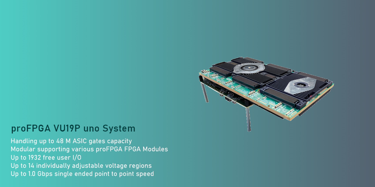
    Equipped with one Xilinx Virtex UltraScale+TM VU19P FPGA module, the proFPGA uno system can handle up to 48 M ASIC gates on the board.

    Very User Friendly

    The proFPGA prototyping system provides an extensive set of features and tools, like remote system configuration, integrated self and performance test, automatic board detection, automatic I/O voltage programming, system scan and safety mechanism, which simplifies the usage of the FPGA based system tremendously.

    Specification

    • FPGA type: Xilinx Virtex UltraScale+ VU19P based FPGA modules  
    • Capacity: Up to 48 M ASIC gates on one board  
    • FPGA-internal memory: Up to 75,9 Mbits on one board  
    • Signaling rate: Up to 14 Extension sites with high speed connectors
    • Extension sites: Up to 1.0 Gbps (standard I/O)/ up to 28 Gbps (MGT)   
    • I/O resources:
      6 x 153 I/Os and 2 x 48 I/Os to top side connectors
      6 x 153 I/Os bottom side connectors  
    • High Speed I/O transceivers: 48 MGTs (up to 28 Gbps)
    • Voltage regions :14 individually adjustable
    • I/O voltage regions: Stepless from 1.2V up 1.8V / Automated detection of daughter cards and setting of right voltages  
    • Configuration: With host software via Ethernet, USB 3.0 or standalone over USB stick 
    • Clock Management
      6 fixed global clock and sync inputs per connector
      use of up to 6 clock-capable I/Os per connector

    System Architechture


    Configuration

    proFPGA uno Xilinx Virtex UltraScale+ 19P based FPGA Prototyping System

    Extension Sites

    14

    FPGA Modules

    1

    FPGAType

    Xilinx Virtex UltraScale+ VU19P

    Logic Capacity (ASIC Gates)

    48 M

    FPGA Memory

    75,9 Mbits

    I/O Resources

    1932

    High Speed I/O Transceivers

    48

    Adjustable Voltage Regions

    14

    Clock Generators

    8 fixed clocks

    Order Code

    PROF-UNO-XCVU19P


    011 yes 128   產品文件:
    20171115 04   產品編號:PROF-UNO-XCVU19P


    Previous Next

    Intel Arria 10 系列 │ quad A10 GX1150 套裝系統

    Product Summary

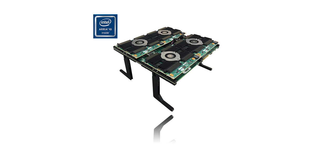
    The proFPGA quad A10 GX1150 system is a complete and modular multi- FPGA solution, which meets highest requirements in the area of FPGA based Prototyping. It addresses customers who need a scalable and flexible high speed ASIC Prototyping solution for early software development and real time system verification. The innovative system concept offers highest flexibility and reusability reconfigurability for several projects, which guarantees the best return on investment.

    Highest Flexibility
    The system architecture is based on a modular and scalable single-chip concept. The FPGAs are assembled on dedicated FPGA modules, which will be plugged on the proFPGA uno, duo or quad motherboard. This offers the highest flexibility to use for example different FPGA types in one system or to scale a system in increments of one FPGA. The user has access to almost all I/Os of the FPGA, which gives him maximum freedom regarding the FPGA interconnection structure. This way the prototyping system can be adapted in the best way to any user design. Furthermore the system offers a total of 32 extension sites on the top and bottom site for standard or user specific extension boards like DDR4 memory, PCIe gen1/2/3, Gigabit Ethernet, USB 3.0 or other high speed interface and interconnect boards.

    Maximum Performance
    The well designed boards of the proFPGA system are optimized and trimmed to guarantee best signal integrity and to achieve highest performance. The high speed boards together with specific high speed connectors allow a maximum point-to-point speed of up to 1.0 Gbps single ended over the standard FPGA I/Os and up to 17.4 Gbps differential over the high speed serial transceivers of the FPGA. This performance combined with the high interconnection flexibility allows the designer to run his design at the highest possible speed on the proFPGA system.

    Biggest Capacity
    Equipped with up to four Intel® Arria® 10 FPGA modules, the proFPGA quad system can handle up to 32 M ASIC gates on only one board. Due to the fact, that multiple proFPGA quad or duo systems can be connected to even larger systems, there is an unlimited scalability and no theoretical maximum in capacity.

    Very User Friendly
    The proFPGA prototyping system provides an extensive set of features and tools, like remote system configuration, integrated self and performance test, automatic board detection, automatic I/O voltage programming, system scan and safety mechanism, which simplifies the usage of the FPGA based system tremendously.

    Specification 

    FPGAs

    • Up to 4 x Intel® Arria® 10 GX1150 FPGA Modules
       

    Capacity

    • Up to 32 M ASIC gates on one board (8 M ASIC gates per FPGA Module)
       

    FPGA-internal memory

    • Up to 217,04 Mbit on one board (54,26 Mbit per FPGA Module)
       

    Signaling rate

    • Up to 1.0 Gbps single ended (standard I/O)/ up to 17.4 Gbps differential
       

    Extension sites

    • Up to 24 extension sites with high speed connectors
       

    I/O resources

    • Overall 2584 signals for I/O and inter FPGA connection
      • 646 free I/Os per FPGA Module
        • 4x141 I/Os to top side connectors
        • 1x43 I/Os and 1x39 to bottom side connectors
    • Single-ended or differential
       

    High Speed I/O transceivers

    • 192 dedicated high speed serial transceivers running up to 17.4 Gbps
      • 48 high speed serial transceivers per FPGA Module
         

    FPGAs interconnections

    • Flexible via high-speed interconnection boards or cables
       

    Voltage regions

    • 24 individually adjustable I/O voltage regions
    • 6 individually adjustable voltage regions per FPGA Module
    • Stepless from 1.2 up 1.8V
    • Automated detection of daughter card and adjustment of right voltage
       

    Configuration

    • Flexible via high-speed interconnection boards or cables
       

    Voltage Regions

    • 24 individually adjustable I/O voltage regions
    • 6 individually adjustable voltage regions per FPGA Module
    • Stepless from 1.2V up to 1.8V on 6 extension sites
    • Automated detection of daughter card and adjustment of right voltage

    Clocking

    • 48 differential external clock inputs
      • 24 differential clock inputs per FPGA Module
      • 6 differential clock inputs per connector
    • Run-time configurable local clocks
      • 8 global clock and sync signal inputs per motherboard
      • Fully synchronous derived clocks with sync signals
         

    Configuration

    • With host software via Ethernet, USB 2.0, PCIe or standalone over USB stick or JTAG
       

    Data exchange

    • On board DMBI (Device Message Box Interface)
    • Data exchange rate:
      • Ethernet (up to 100 Mbps)
      • USB (480 Mbps)
      • PCIe (up to 3.5 Gbps)
         

    Power

    • External (optional) ATX Power Supply (12 V, 24 - 35 A output)
       

    Dimensions

    • 5.91" x 0.95" x 12.20" / 150 mm x 24 mm x 310 mm (width x height x depth)
    • 1.5 kg weight

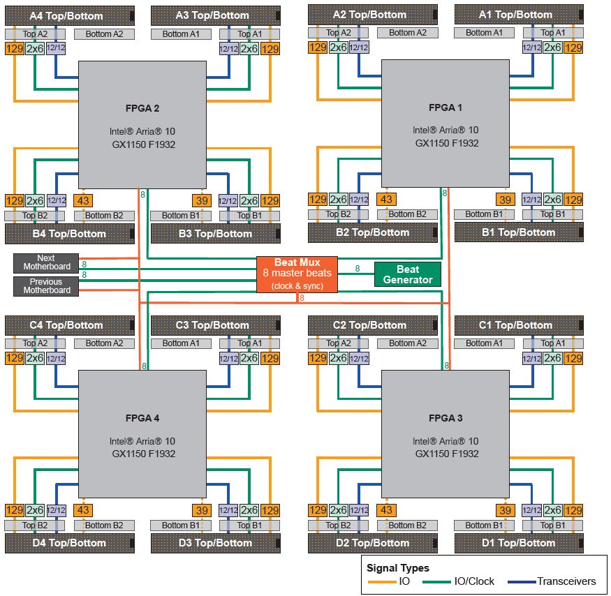
    System Architechture 


    Configurations 

    proFPGA quad Intel®Arria® 10 GX1150 FPGA Prototyping System Configurations
      proFPGA quad A10 GX1150 FM1 proFPGA quad A10 GX1150 FM2 proFPGA quad A10 GX1150 FM3 proFPGA quad A10 GX1150 FM4
    Extension Sites 6 12 18 24
    FPGA Modules 1 2 3 4
    FPGAType Intel® Arria® 10 GX1150 F1932 Intel® Arria® 10 GX1150 F1932 Intel® Arria® 10 GX1150 F1932 Intel® Arria® 10 GX1150 F1932
    Logic Capacity (ASIC Gates) 8M 16M 24M 32M
    FPGA Memory 54,26 Mbit 108,62 Mbit 162,78 Mbit 217,04 Mbit
    I/O Resources 646 1292 1938 2584
    High Speed I/O Transceivers 48 96 144 192
    Adjustable Voltage Regions 6 12 18 24
    Interconnections flexible flexible flexible flexible
    Clock Inputs 54 + 6 108 + 6 162 + 6 216 + 6
    Global Clocks 8/x-derived 8/x-derived 8/x-derived 8/x-derived
    Order Code PROF-QUAD-A10GX115-FM1 PROF-QUAD-A10GX115-FM2 PROF-QUAD-A10GX115-FM3 PROF-QUAD-A10GX115-FM4


    011 yes 128   產品文件:產品型錄(EN) │ proFPGA 產品總覽 (EN)
    20171115 04   產品編號:PROF-QUAD-A10GX115-FM1, PROF-QUAD-A10GX115-FM2, PROF-QUAD-A10GX115-FM3, PROF-QUAD-A10GX115-FM4


    和澄科技 Haley Technology

    電話 │ 886-3-5790380
    傳真 │ 886-3-5790370
    信箱 │ sales@haleytech.com
    地址 │ 新竹市關新路27號18樓之2


    M有任何問題嗎? Line 我們最快! 

    產品搜尋